- 您现在的位置:买卖IC网 > Sheet目录3850 > AT89C51CC03C-S3SIM (Atmel)IC 8051 MCU FLASH 64K 52PLCC
132
AT89C51CC03
4182O–CAN–09/08
When the Master device transmits data to the Slave device via the MOSI line, the Slave
device responds by sending data to the Master device via the MISO line. This implies
full-duplex transmission with both data out and data in synchronized with the same clock
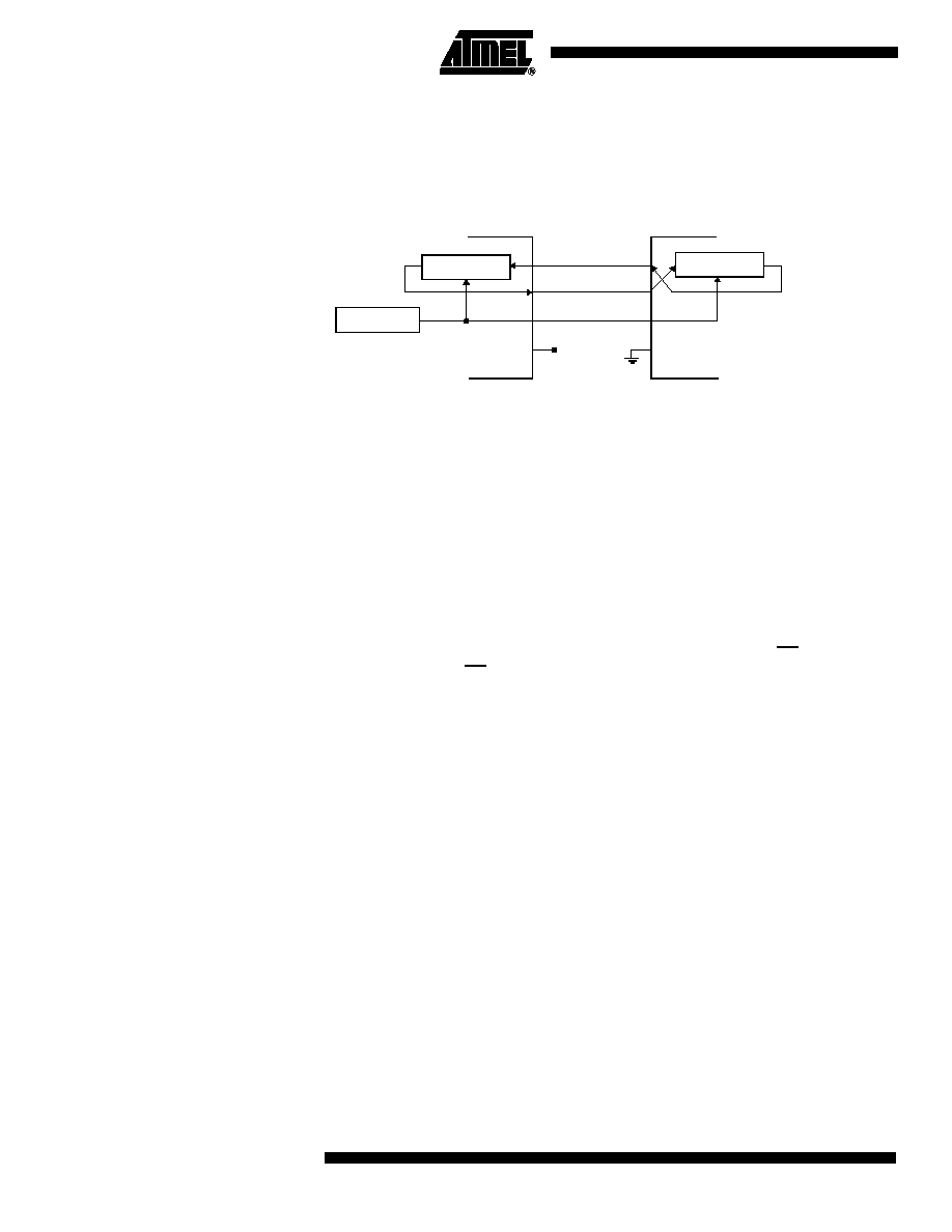
Figure 59. Full-Duplex Master-Slave Interconnection
Master Mode
The SPI operates in Master mode when the Master bit, MSTR (1), in the SPCON register
is set. Only one Master SPI device can initiate transmissions. Software begins the trans-
mission from a Master SPI Module by writing to the Serial Peripheral Data Register
(SPDAT). If the shift register is empty, the Byte is immediately transferred to the shift
register. The Byte begins shifting out on MOSI pin under the control of the serial clock,
SCK. Simultaneously, another Byte shifts in from the Slave on the Master’s MISO pin.
The transmission ends when the Serial Peripheral transfer data flag, SPIF, in SPSCR
becomes set. At the same time that SPIF becomes set, the received Byte from the Slave
is transferred to the receive data register in SPDAT. Software clears SPIF by reading
the Serial Peripheral Status register (SPSCR) with the SPIF bit set, and then reading the
SPDAT.
Slave Mode
The SPI operates in Slave mode when the Master bit, MSTR (2), in the SPCON register is
cleared. Before a data transmission occurs, the Slave Select pin, SS, of the Slave
device must be set to’0’. SS must remain low until the transmission is complete.
In a Slave SPI Module, data enters the shift register under the control of the SCK from
the Master SPI Module. After a Byte enters the shift register, it is immediately trans-
ferred to the receive data register in SPDAT, and the SPIF bit is set. To prevent an
overflow condition, Slave software must then read the SPDAT before another Byte
enters the shift register (3). A Slave SPI must complete the write to the SPDAT (shift reg-
ister) at least one bus cycle before the Master SPI starts a transmission. If the write to
the data register is late, the SPI transmits the data already in the shift register from the
previous transmission.
Transmission Formats
Software can select any of four combinations of serial clock (SCK) phase and polarity
using two bits in the SPCON: the Clock Polarity (CPOL (4)) and the Clock Phase
(CPHA4). CPOL defines the default SCK line level in idle state. It has no significant
effect on the transmission format. CPHA defines the edges on which the input data are
sampled and the edges on which the output data are shifted (Figure 60 and Figure 61).
The clock phase and polarity should be identical for the Master SPI device and the com-
municating Slave device.
8-bit Shift register
SPI
Clock Generator
Master MCU
8-bit Shift register
MISO
MOSI
SCK
VSS
VDD
SS
Slave MCU
1.
The SPI Module should be configured as a Master before it is enabled (SPEN set). Also,
the Master SPI should be configured before the Slave SPI.
2.
The SPI Module should be configured as a Slave before it is enabled (SPEN set).
3.
The maximum frequency of the SCK for an SPI configured as a Slave is the bus clock
speed.
4.
Before writing to the CPOL and CPHA bits, the SPI should be disabled (SPEN =’0’).
发布紧急采购,3分钟左右您将得到回复。
相关PDF资料
AT89C51CC03C-RLTIM
IC 8051 MCU FLASH 64K 44VQFP
AT89C51CC03C-7CTIM
IC 8051 MCU FLASH 64K 64BGA
AT89C5132-ROTIL
IC 8051 MCU FLASH 64K USB 80TQFP
PIC18F46K80-I/P
MCU PIC 64KB FLASH 40DIP
AT89C5131A-RDTIL
IC 8051 MCU FLASH 32K USB 64VQFP
PIC24EP64GP202-I/SP
MCU 16BIT 64KB FLASH 28SPDIP
PIC24EP64MC202-I/SP
MCU 16BIT 64KB FLASH 28SPDIP
PIC18LF26J53-I/SP
IC PIC MCU 64KB FLASH 28SPDIP
相关代理商/技术参数
AT89C51CC03C-SLRIM
功能描述:IC 8051 MCU FLASH 64K 44PLCC RoHS:否 类别:集成电路 (IC) >> 嵌入式 - 微控制器, 系列:AT89C CAN 标准包装:1,500 系列:AVR® ATtiny 核心处理器:AVR 芯体尺寸:8-位 速度:16MHz 连通性:I²C,LIN,SPI,UART/USART,USI 外围设备:欠压检测/复位,POR,PWM,温度传感器,WDT 输入/输出数:16 程序存储器容量:8KB(4K x 16) 程序存储器类型:闪存 EEPROM 大小:512 x 8 RAM 容量:512 x 8 电压 - 电源 (Vcc/Vdd):2.7 V ~ 5.5 V 数据转换器:A/D 11x10b 振荡器型:内部 工作温度:-40°C ~ 125°C 封装/外壳:20-SOIC(0.295",7.50mm 宽) 包装:带卷 (TR)
AT89C51CC03C-SLSIM
制造商:ATMEL 制造商全称:ATMEL Corporation 功能描述:Enhanced 8-bit MCU with CAN Controller and Flash Memory
AT89C51CC03U-7CTIM
功能描述:IC 8051 MCU FLASH 64K 64BGA RoHS:否 类别:集成电路 (IC) >> 嵌入式 - 微控制器, 系列:AT89C CAN 标准包装:9 系列:87C 核心处理器:8051 芯体尺寸:8-位 速度:40/20MHz 连通性:UART/USART 外围设备:POR,WDT 输入/输出数:32 程序存储器容量:32KB(32K x 8) 程序存储器类型:OTP EEPROM 大小:- RAM 容量:256 x 8 电压 - 电源 (Vcc/Vdd):4.5 V ~ 5.5 V 数据转换器:- 振荡器型:内部 工作温度:0°C ~ 70°C 封装/外壳:40-DIP(0.600",15.24mm) 包装:管件
AT89C51CC03UA-7CTUM
制造商:Rochester Electronics LLC 功能描述: 制造商:Atmel Corporation 功能描述:
AT89C51CC03UA-RDTUM
功能描述:8位微控制器 -MCU CAN C51 64K FLASH UAR BOOT RoHS:否 制造商:Silicon Labs 核心:8051 处理器系列:C8051F39x 数据总线宽度:8 bit 最大时钟频率:50 MHz 程序存储器大小:16 KB 数据 RAM 大小:1 KB 片上 ADC:Yes 工作电源电压:1.8 V to 3.6 V 工作温度范围:- 40 C to + 105 C 封装 / 箱体:QFN-20 安装风格:SMD/SMT
AT89C51CC03UA-RDTZM
制造商:ATMEL 制造商全称:ATMEL Corporation 功能描述:Enhanced 8-bit MCU with CAN Controller and Flash Memory
AT89C51CC03UA-RLTUM
功能描述:8位微控制器 -MCU CAN C51 64K FLASH UAR BOOT RoHS:否 制造商:Silicon Labs 核心:8051 处理器系列:C8051F39x 数据总线宽度:8 bit 最大时钟频率:50 MHz 程序存储器大小:16 KB 数据 RAM 大小:1 KB 片上 ADC:Yes 工作电源电压:1.8 V to 3.6 V 工作温度范围:- 40 C to + 105 C 封装 / 箱体:QFN-20 安装风格:SMD/SMT
AT89C51CC03UA-RLTZM
制造商:ATMEL 制造商全称:ATMEL Corporation 功能描述:Enhanced 8-bit MCU with CAN Controller and Flash Memory